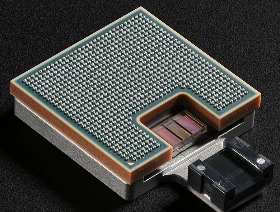
IBM is developing co-packaged optics technology to enable faster chip communication, improved energy efficiency and longer data centre interconnect cables.
Technology giant IBM has unveiled breakthrough research into optics technology that could stand to dramatically improve how data centres train and run generative AI (Gen AI) models.
The company’s co-packaged optics innovation could replace electrical interconnects in data centres to offer significant improvements in speed and energy efficiency for AI and other computing applications.
Researchers have pioneered a new process for co-packaged optics (CPOs), the next generation of optics technology, to enable connectivity within data centres at the speed of light.

By designing and assembling the first publicly announced successful polymer optical waveguide (PWG) to power this technology, IBM researchers have shown how CPO will redefine the way the computing industry transmits high-bandwidth data between chips, circuit boards and servers.
Enabling high-speed optical connectivity
Fibre optic technology is able to carry data at high speeds across long distances. It manages nearly all the world’s commerce and communications traffic with light instead of electricity.
Whilst data centres use fibre optics for their external communications networks, racks in data centres still predominantly run communications on copper-based electrical wires. The wires connect GPU accelerators that may spend a lot of time idle and wait for data from other devices, which can incur significant expense and energy.
THIS RESEARCH INNOVATION, AS DESCRIBED, WOULD ENABLE:
- Lower costs for scaling Gen AI through a more than 5x power reduction in energy consumption
- Extending the length of data centre interconnect cables from one to hundreds of metres
- Faster AI model training so that developers can train LLMs up to five times faster
- Saving the energy equivalent of 5,000 US homes, dramatically increasing energy efficiency for data centres
IBM researchers have demonstrated a way to bring optics’ speed and capacity inside data centres. In a newly published paper, IBM introduced a new CPO prototype module that can enable high-speed optical connectivity.
According to IBM, this technology could significantly increase the bandwidth of data centre communications, thereby minimising GPU downtime and accelerating AI processing.
“As Gen AI demands more energy and processing power, the data centre must evolve – and co-packaged optics can make these data centres future-proof,” says Dario Gil, SVP and Director of Research at IBM.
Boosting bandwidth between chips
In recent years, advances in chip technology have densely packed transistors onto a chip. IBM says that CPO technology aims to “scale the interconnection density between accelerators by enabling chipmakers to add optical pathways connecting chips on an electronic module beyond the limits of today’s electrical pathways”.
IBM suggests that new high bandwidth density optical structures – when coupled with transmitting multiple wavelengths per optical channel – have the potential to boost bandwidth between chips as much as 80 times, compared to electrical connections.
Such an innovation could enable chipmakers to add six times as many optical fibres at the edge of a silicon photonics chip. Each fibre, about three times the width of a human hair, could span centimetres to hundreds of meters in length and transmit terabits of data per second.
Dario adds: “With this breakthrough, tomorrow’s chips will communicate much like how fibre optics cables carry data in and out of data centres, ushering in a new era of faster, more sustainable communications that can handle the AI workloads of the future.”


